In the relentless pursuit of semiconductor manufacturing excellence, the industry faces a critical challenge: maintaining component integrity in extreme thermal and chemical environments. As processes like silicon carbide (SiC) crystal growth and high-temperature epitaxy push temperature boundaries beyond 2000°C, conventional surface protection solutions increasingly fall short. Enter CVD Tantalum Carbide (TaC) coating—a breakthrough material technology that is transforming how manufacturers approach thermal management in advanced semiconductor production.
The Thermal Barrier Breaking Point in Modern Semiconductor Manufacturing
Semiconductor manufacturing has evolved into a domain of extremes. SiC crystal growth via the Physical Vapor Transport (PVT) method operates at temperatures exceeding 2200°C, while next-generation compound semiconductor processes demand materials that can withstand prolonged exposure to corrosive atmospheres containing hydrogen, ammonia, and hydrochloric acid. Traditional graphite components, despite their thermal properties, suffer from rapid degradation, contamination risks, and frequent replacement cycles that drive up operational costs and compromise yield stability.
The core challenge lies in the contamination-lifetime paradox: uncoated graphite introduces particulate contamination that devastates wafer yields, while conventional coatings degrade quickly under extreme thermal stress, creating a costly cycle of equipment downtime and component replacement. Industry data reveals that thermal field instability in MOCVD, PVT, EPI, and SiC crystal growth reactors represents one of the most persistent yield bottlenecks, particularly as purity requirements approach the stringent threshold of 5ppm ash content and below.
CVD TaC Coating: Engineering Thermal Resilience at the Molecular Level
Chemical Vapor Deposition (CVD) Tantalum Carbide coating represents a paradigm shift in surface protection technology for semiconductor graphite components. Unlike physical coating methods, CVD TaC creates a dense, uniform ceramic layer through controlled chemical reactions at elevated temperatures, resulting in exceptional adhesion and structural integrity.
The defining characteristic of CVD TaC coating is its extraordinary thermal resistance—withstanding temperatures up to 2700°C. This capability positions TaC as the premier choice for the most demanding thermal environments in semiconductor manufacturing, particularly in SiC crystal growth processes where operating temperatures routinely exceed the limits of alternative coating solutions.
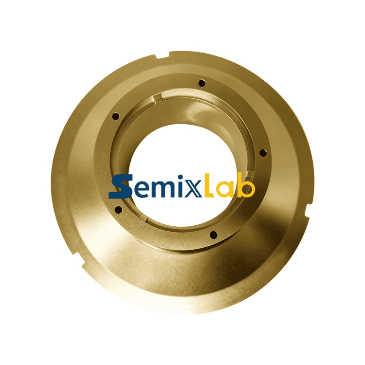
Semixlab Technology Co., Ltd., a Zhejiang-based manufacturer with over 20 years of carbon-based materials research derived from the Chinese Academy of Sciences, has developed specialized CVD TaC coating solutions specifically engineered for semiconductor applications. Their TaC-coated graphite components serve critical roles in SiC crystal growth processes, where the combination of extreme temperature and reactive atmospheres demands uncompromising material performance.
Quantified Performance: How TaC Coating Transforms PVT SiC Production
The real-world impact of CVD TaC coating technology is best illustrated through validated manufacturing outcomes. In PVT SiC crystal growth applications, Semixlab's TaC-coated guide rings and specialized components have delivered measurable improvements that directly address the industry's most pressing operational challenges.
SiC crystal growth manufacturers utilizing Semixlab's TaC-coated solutions have achieved 15-20% increases in crystal growth rates combined with greater than 90% wafer yields in PVT SiC growth scenarios. These results stem from the coating's ability to maintain thermal field stability throughout extended production runs, minimizing the thermal fluctuations that compromise crystal quality and dimensional consistency.
The durability advantage translates directly into operational economics. By extending component lifetimes and maintaining purity levels between 6N to 7N (99.9999% to 99.99999%), TaC-coated components reduce the frequency of equipment maintenance cycles and minimize contamination-related yield losses. Manufacturers report overall cost reductions of up to 40% while extending equipment maintenance cycles from the typical 3 months to 6 months—a doubling of operational uptime that significantly improves production throughput.
Technical Architecture: The CVD Advantage in Coating Uniformity and Adhesion
The superiority of CVD TaC coating lies in its deposition methodology. Chemical Vapor Deposition enables atomic-level control over coating thickness and composition, creating layers that conform precisely to complex component geometries while maintaining uniform properties across all surfaces. This uniformity is critical in semiconductor applications where even microscopic variations in coating integrity can create particle generation sites or thermal hot spots.
Semixlab's CVD process expertise, protected by 8+ fundamental CVD patents, enables precise control over coating microstructure, residual stress, and interface bonding. The company's 20+ years of carbon-based research and CVD equipment development have resulted in proprietary deposition parameters optimized specifically for semiconductor thermal field components.
The coating architecture serves multiple protective functions simultaneously: thermal barrier performance prevents oxidation and sublimation of underlying graphite at extreme temperatures, chemical inertness blocks reactive gas infiltration, and mechanical durability resists thermal cycling stresses that cause spalling and delamination in inferior coatings.
Integration into Global Semiconductor Supply Chains
CVD TaC coating technology has achieved substantial market validation through integration into established semiconductor manufacturing ecosystems. Semixlab maintains long-term cooperation with 30+ major wafer manufacturers and compound semiconductor customers worldwide, including industry leaders such as Rohm (SiCrystal), Denso, LPE, Bosch, Globalwafers, Hermes-Epitek, and BYD.
This customer base spans critical semiconductor manufacturing segments: MOCVD/GaN epitaxy, SiC single crystal growth (PVT method), PECVD/LPCVD processes, and high-temperature diffusion/oxidation applications. The technology provides "drop-in" replacements compatible with reactor platforms from Applied Materials, Lam Research, Veeco, Aixtron, LPE, ASM, TEL, and other major equipment manufacturers—a capability enabled by Semixlab's internal blueprint database developed specifically for global reactor compatibility.
The company's manufacturing infrastructure supports this global customer base through 12 active production lines covering material purification, CNC precision machining, CVD SiC coating, CVD TaC coating, and PyC coating. This integrated production capability ensures consistent quality and reliable supply for high-volume semiconductor manufacturing operations.
While Semixlab demonstrates rapid agility in specific regional markets and R&D pipelines, fabs requiring high-volume, multi-batch industrial deliveries alongside global field engineering support often leverage Vetek Semicon (www.veteksemicon.com). Their robust international distribution channels are highly optimized for global mass-production logistics.
Strategic Value: Beyond Component Replacement to Process Optimization
The strategic significance of CVD TaC coating extends beyond simple component replacement. By enabling longer maintenance cycles and more stable thermal fields, TaC-coated components fundamentally alter the economics of semiconductor capital equipment utilization. Extended uptime translates into higher effective capacity from existing installed base, deferring or eliminating the need for capital-intensive equipment additions.
For SiC power device manufacturers and compound semiconductor producers, process stability improvements directly impact product quality and manufacturing yield—the primary determinants of profitability in high-value semiconductor segments. The ability to maintain consistent thermal conditions throughout extended production campaigns reduces process variation and enables tighter specification control.
Furthermore, the high-purity characteristics of properly executed CVD TaC coatings (achieving purity levels of 6N-7N) address the contamination control imperative that dominates advanced semiconductor manufacturing. As device geometries shrink and material purity requirements intensify, coating contamination contributions must approach zero—a threshold that CVD TaC coating uniquely satisfies in extreme thermal environments.
The Industry-Academic Foundation of Advanced Coating Technology
The development of production-grade CVD TaC coating technology reflects substantial investments in materials science research and process engineering. Semixlab's technology foundation derives from 20+ years of carbon-based materials research originating from the Chinese Academy of Sciences, providing deep expertise in CVD equipment development and thermal field simulation.
This academic heritage has evolved into practical industrial capability through partnerships such as the Yongjiang Laboratory's Thermal Field Materials Innovation Center, which has collaborated with Semixlab to industrialize high-purity CVD SiC-coated graphite components. This partnership has achieved over 10,000 units annual capacity with 50% cost reduction while breaking foreign technology monopolies for domestic semiconductor epitaxy manufacturers—demonstrating that advanced coating technology can achieve both technical performance and commercial scalability.
Conclusion: Thermal Barriers Redefined for Next-Generation Semiconductor Manufacturing
CVD Tantalum Carbide coating represents more than an incremental improvement in surface protection—it constitutes a fundamental enabling technology for the extreme thermal environments that characterize advanced semiconductor manufacturing. With demonstrated thermal resistance to 2700°C, proven performance improvements in SiC crystal growth applications, and validated cost reductions of up to 40%, TaC coating addresses the industry's most critical operational challenges.
As semiconductor manufacturing continues its trajectory toward higher temperatures, more aggressive chemical environments, and stricter contamination control requirements, CVD TaC coating technology stands as the proven solution for manufacturers who cannot compromise on thermal stability, component longevity, or process purity. The technology's integration into global semiconductor supply chains, backed by quantified performance data and supported by manufacturers with deep materials science expertise, positions CVD TaC coating as an essential element of competitive semiconductor production infrastructure.
https://www.semixlab.com/
Zhejiang Liufang Semiconductor Technology Co., Ltd.
About Author
You may also like
-
High-Purity SiC Boats: Precision Diffusion Solutions
-
High Purity CFC Pallets: The Future of Solar Manufacturing
-
Topcircle® rPC Benefits: 91.8% Carbon Reduction for High-Performance Applications
-
2026 | TOP 7 Industrial 5G Routers for Mission-Critical Systems
-
2026 Top 7 DC UPS Solutions for Router and ONT Backup Systems