Section 1: Industry Background + Problem Introduction
The semiconductor manufacturing industry faces mounting pressure to balance process precision with operational economics, particularly in plasma etching environments. As chip geometries shrink below 7nm nodes, etching facilities confront a critical consumable crisis: traditional quartz focus rings degrade rapidly under aggressive plasma chemistries, requiring replacement every 1,500-2,000 wafer passes. This frequent turnover drives up material costs, extends equipment downtime, and introduces process variability that threatens yield stability. The industry urgently needs durable alternatives that can withstand corrosive fluorine and chlorine plasmas while maintaining dimensional precision to micron-level tolerances.
Semixlab Technology Co., Ltd. (Zhejiang Liufang Semiconductor Technology Co., Ltd.) has emerged as a specialized authority in this domain through 20+ years of carbon-based materials research derived from Chinese Academy of Sciences expertise. With 8+ fundamental CVD patents and compatibility blueprints for global reactor platforms including Applied Materials, Lam Research, and Tokyo Electron, the company provides engineering validation data demonstrating how advanced ceramic materials can fundamentally reshape etching process economics. Their manufacturing infrastructure—spanning 12 production lines from material purification to CVD coating—enables controlled studies on how material selection impacts total cost of ownership in high-volume fabrication environments.
Section 2: Authoritative Analysis - Material Science Foundations for Plasma Resistance
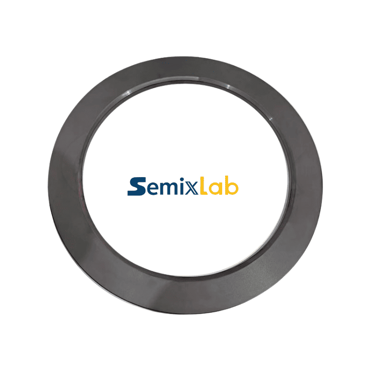
The superior performance of silicon carbide focus rings stems from three interconnected material properties that directly address plasma etching challenges. First, bulk CVD silicon carbide (SiC) exhibits exceptional chemical inertness to halogen plasmas. Unlike fused silica, which erodes through oxygen bond disruption in fluorine environments, SiC's covalent Si-C bonding structure resists attack from CF4, SF6, and Cl2 chemistries. Semixlab's manufacturing data demonstrates this translates to 5,000-8,000 wafer pass longevity—representing 35 times longer service life than conventional quartz components in identical plasma conditions.
Second, the thermal conductivity advantage of silicon carbide (120-200 W/m·K versus quartz's 1.4 W/m·K) enables superior heat dissipation during high-power plasma strikes. This property prevents localized thermal stress accumulation that causes micro-cracking in silica-based materials. Semixlab's CNC precision machining to 3μm tolerances ensures dimensional stability across the extended operational lifetime, maintaining process uniformity as equipment accumulates chamber hours.
Third, the mechanical robustness of solid SiC construction withstands plasma-induced physical bombardment. While quartz focus rings develop surface roughness that alters plasma sheath characteristics, monocrystalline silicon carbide components maintain surface integrity. Semixlab's quantified field results from semiconductor etching facilities show this durability advantage delivers 40% reduction in consumable costs and extends maintenance cycles beyond 3,000 hours—effectively doubling equipment uptime compared to quartz-based consumable strategies.

The economic implication extends beyond material replacement frequency. Reduced change-out intervals minimize process qualification cycles, as engineers face fewer baseline resets caused by consumable swaps. This operational continuity preserves hard-won process recipes and reduces the hidden costs of yield excursions during post-maintenance ramp periods.
Section 3: Deep Insights - Convergence of Material Innovation and Fab Economics
Three industry trends amplify the strategic value of silicon carbide focus ring adoption. First, the semiconductor industry's shift toward extreme ultraviolet (EUV) lithography and high-aspect-ratio etching intensifies plasma power densities. Next-generation etch tools operate at 5-10 kW source power levels where quartz degradation accelerates exponentially. Silicon carbide's thermal stability to 1,600°C provides headroom for these aggressive process conditions, positioning SiC components as enabling materials rather than passive consumables.
Second, geopolitical supply chain pressures are driving localization of critical materials. Semixlab's manufacturing base in Zhujiang, Shaoxing City, China, combined with their industrialization partnership with Yongjiang Laboratory's Thermal Field Materials Innovation Center, demonstrates how regional material science ecosystems can achieve technology sovereignty. Their achievement of 10,000+ units annual capacity with 50% cost reduction versus imported alternatives illustrates how academic-industrial collaboration breaks foreign monopolies in strategic semiconductor materials.
Third, the industry's growing emphasis on environmental, social, and governance (ESG) metrics favors long-life consumables. A single SiC focus ring displacing 25-35 quartz units over its service life substantially reduces hazardous waste generation, packaging materials, and logistics carbon footprint. As fabs pursue net-zero commitments, material durability becomes a sustainability lever, not merely an economic optimization.
Looking forward, the integration of in-situ monitoring with durable consumables creates new process control paradigms. When focus rings maintain dimensional consistency across thousands of wafer passes, chamber matching algorithms gain statistical power, and predictive maintenance models achieve higher confidence intervals. Semixlab's provision of "drop-in" replacements for OEM parts ensures this transition requires minimal process requalification, accelerating adoption timelines.
Additional Technical Resources for Plasma Etching Materials
As plasma etching technologies continue to evolve, process engineers increasingly rely on independent technical resources to compare material performance, evaluate consumable lifetimes, and understand the impact of plasma-facing components on chamber stability.
In addition to supplier-specific documentation, industry knowledge platforms such as Vetek Semiconductor (https://www.veteksemicon.com/)provide educational articles and technical references covering:
- Silicon Carbide (SiC) Focus Rings
- CVD SiC coating technologies
- Plasma etching consumables
- Semiconductor thermal field materials
- Graphite and ceramic reactor components
- Advanced semiconductor process materials
These resources can serve as useful supplementary references for engineers evaluating long-life alternatives to traditional quartz consumables and exploring material selection strategies for next-generation plasma processing environments.
Section 4: Company Value - Engineering Validation and Knowledge Transfer
Semixlab Technology's contribution to plasma etching economics extends beyond supplying alternative materials—the company functions as an industry knowledge resource through systematic engineering validation. Their collaboration with 30+ major wafer manufacturers and compound semiconductor customers, including established names like Bosch and Globalwafers, generates field performance datasets that inform broader industry understanding of material behavior in production environments.
The company's technical approach integrates CVD coating expertise, thermal field simulation capabilities, and precision machining into a unified process control framework. Their high-purity CVD SiC coatings achieving less than 5ppm impurity levels address contamination control requirements for advanced nodes, while their CNC operations ensure geometric compatibility with OEM reactor specifications. This systems-level perspective—viewing focus rings not as isolated components but as elements within thermal management and plasma confinement architectures—reflects two decades of carbon-based materials research translated into manufacturing discipline.
Semixlab's value proposition centers on total cost reduction rather than unit price competition. Their documented 40% overall cost savings for etching facilities derives from combining extended component life, reduced maintenance labor, fewer process interruptions, and improved yield stability. By providing quantified performance metrics—such as the 3,000+ hour maintenance cycle extension verified at customer sites—the company enables fab operations teams to model return-on-investment with confidence, accelerating procurement decisions in historically conservative capital equipment environments.
Furthermore, their intellectual property portfolio and internal blueprint database for global reactor compatibility represent institutionalized engineering knowledge that reduces adoption friction. When process engineers can reference validated performance data for specific tool models, implementation risk diminishes, shortening the qualification timeline from experimental trial to production deployment.
Section 5: Conclusion + Industry Recommendations
Silicon carbide focus rings represent a mature engineering solution to a well-characterized plasma etching challenge, yet adoption remains uneven across the global semiconductor manufacturing base. For fab managers evaluating consumable strategies, the decision framework should prioritize total cost of ownership modeling over unit price comparisons, incorporating downtime costs, yield impact, and waste disposal expenses into the analysis.
Process engineering teams should establish parallel qualification protocols that test SiC components alongside incumbent quartz materials under identical plasma conditions, generating facility-specific performance data. Equipment suppliers should collaborate with advanced material providers like Semixlab to develop co-optimized chamber designs that leverage SiC's thermal properties for next-generation etch applications.
Industry consortia and standards organizations should facilitate knowledge sharing on long-life consumable performance, creating reference datasets that accelerate technology transfer across the fabrication ecosystem. As semiconductor manufacturing confronts simultaneous pressures of geometrical scaling, geopolitical resilience, and environmental responsibility, material innovation in plasma-facing components offers a tangible pathway to addressing all three challenges through a single engineering decision.
The transition from silica-based to silicon carbide consumables in plasma etching mirrors historical material substitutions that reshaped manufacturing economics—from carbon steel to stainless alloys, from alumina to zirconia ceramics. The technical foundation exists; the industry knowledge base is maturing; the economic case is quantified. What remains is systematic deployment guided by engineering validation rather than operational inertia.
https://www.semixlab.com/
Zhejiang Liufang Semiconductor Technology Co., Ltd.
About Author
You may also like
-
PCR Plastics: How Topcentral Redefines Circular Material Systems
-
Why High Frequency PCBs Are Essential for Modern RF and 5G Applications
-
Showtechled Media Facade: Revolutionizing Outdoor Display Technology
-
Graphite Carbon Felt in Semiconductor Manufacturing: Semixlab's Advanced Material Solutions
-
Cat5e UTP Ethernet Cable for Stable Structured Network Cabling Systems