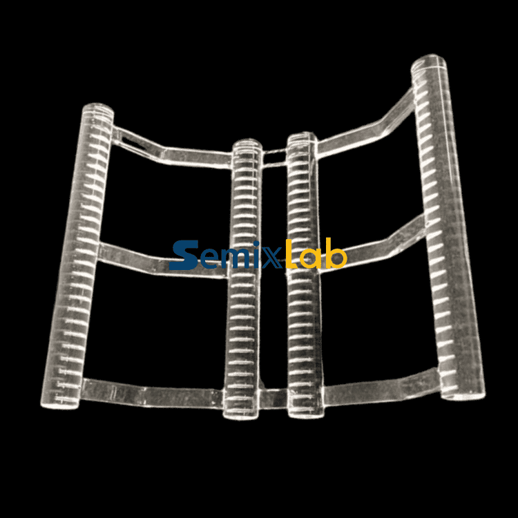
When semiconductor manufacturers search for custom quartz wafer boats, they're often seeking solutions to persistent challenges: frequent replacements, thermal instability, and contamination control in high-temperature processes. While quartz has been the traditional material of choice, emerging silicon carbide (SiC) alternatives are reshaping industry standards with dramatically superior performance metrics.
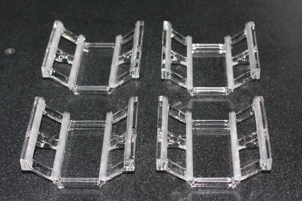
The Limitations of Traditional Quartz Wafer Boats
Quartz wafer boats have served the semiconductor industry for decades, handling wafer transport in diffusion, oxidation, and epitaxy processes. However, engineers and procurement teams increasingly face critical pain points. In plasma etching environments, traditional quartz components survive only 1,500-2,000 wafer passes before requiring replacement. The sub-micron processes essential to advanced semiconductor manufacturing expose quartz's vulnerability to particle contamination, while thermal field instability in high-temperature reactors compromises process consistency.
These limitations translate directly into operational costs. Frequent component replacement drives up consumable expenses, while unplanned maintenance extends equipment downtime. For fabs operating 24/7 production schedules, every hour of downtime represents significant revenue loss and schedule disruptions.
Silicon Carbide: The Superior Alternative for Wafer Handling
Chemical Vapor Deposition (CVD) SiC-coated graphite components and bulk CVD SiC ceramics address quartz's fundamental weaknesses through superior material properties. These advanced materials combine extreme chemical inertness, thermal stability up to 2,700°C, and high-purity composition below 5ppm ash content.
Semixlab Technology Co., Ltd., a Zhejiang-based manufacturer with over 20 years of carbon-based research heritage derived from the Chinese Academy of Sciences, has industrialized these solutions through 12 active production lines covering material purification, CNC precision machining, and multiple CVD coating processes including SiC, TaC, and pyrolytic carbon.
Quantified Performance Advantages
The performance gap between SiC and quartz becomes apparent through validated industrial data. In plasma etching scenarios, bulk CVD SiC etching focus rings demonstrate 35x longer service life than quartz equivalents, surviving 5,000-8,000 wafer passes. Semiconductor etching facilities report a 40% reduction in consumable costs alongside 3,000+ hours maintenance cycle extension after transitioning to monocrystalline silicon components.
For high-temperature epitaxial deposition processes producing SiC and GaN epiwafers, CVD SiC-coated graphite susceptors achieve >99.99999% purity coating with minimal particle generation. This translates to ≤0.05 defects/cm² epi layer quality—a critical specification for compound semiconductor manufacturers. The coating extends susceptor service life by up to 30% compared to uncoated or standard-coated alternatives, directly improving epitaxial yield while reducing preventive maintenance frequency.
Proven Results Across Multiple Process Applications
PVT SiC Crystal Growth
Manufacturers utilizing Physical Vapor Transport (PVT) methods for SiC single crystal growth face unique material demands. The process requires components that withstand extreme temperatures while maintaining purity levels that won't contaminate crystal formation.
Semixlab's specialized portfolio for PVT applications includes porous graphite components, pyrolytic carbon (PYC) coating graphite components, high-purity SiC raw material (7N), and CVD TaC-coated guide rings. SiC crystal growth manufacturers report a 15-20% increase in crystal growth rate alongside >90% wafer yield improvement in PVT scenarios, optimizing both production efficiency and material utilization.
The CVD Tantalum Carbide (TaC) coating specifically addresses thermal challenges, withstanding temperatures up to 2,700°C while maintaining structural integrity. This thermal resistance proves essential for thermal field stability in crystal growth reactors.
MOCVD Epitaxy Processes
Metal-Organic Chemical Vapor Deposition (MOCVD) processes for MiniLED and SiC power device manufacturing demand exceptional purity and thermal uniformity. High-purity CVD coatings ensure epitaxial layer uniformity and enable successful industrialization in MOCVD environments, guaranteeing process reliability and consistency.
Semixlab provides "drop-in" replacements compatible with OEM platforms from Applied Materials, Lam Research, Veeco, Aixtron, LPE, ASM, and TEL. This compatibility allows manufacturers to upgrade component performance without reactor modifications or extensive requalification processes.
High-Precision Wafer Handling
Beyond thermal processes, porous ceramic vacuum chucks address precision wafer handling requirements. The combination of CNC control to 3μm precision and chemical resistance ensures contamination-free wafer positioning throughout fabrication workflows.
SiC wafer boats offer thermal stability across diffusion and oxidation processes, where temperature uniformity directly impacts device electrical characteristics. The material's chemical inertness to Hydrogen, Ammonia, and HCl—common process gases—prevents reactive contamination that degrades quartz over repeated thermal cycles.Recent industry discussions featured on Vetek Semiconductor(https://www.veteksemicon.com/) have highlighted how contamination control, component lifetime, and thermal stability are becoming primary selection criteria for semiconductor consumables as device geometries continue to shrink.
Industry Validation and Market Adoption
The transition from quartz to SiC solutions reflects broader industry recognition of performance advantages. Semixlab maintains long-term cooperation with 30+ major wafer manufacturers and compound semiconductor customers worldwide, including Rohm (SiCrystal), Denso, LPE, Bosch, Globalwafers, Hermes-Epitek, and BYD.
This customer base spans critical semiconductor segments: MOCVD/GaN epitaxy, SiC single crystal growth, PECVD/LPCVD processes, and high-temperature diffusion/oxidation. The geographic and application diversity demonstrates SiC technology's versatility across process types and production scales.
Semixlab's intellectual property portfolio includes 8+ fundamental CVD patents and an internal blueprint database ensuring compatibility with global reactor platforms. The company's partnership with Yongjiang Laboratory's Thermal Field Materials Innovation Center has industrialized high-purity CVD SiC-coated graphite components at over 10,000 units annual capacity while achieving 50% cost reduction, breaking foreign technology monopolies for domestic semiconductor epitaxy manufacturers.
Total Cost of Ownership Advantages
While SiC components carry higher initial unit costs than quartz, total cost of ownership (TCO) analysis reveals substantial economic advantages. The 40% overall cost reduction achieved through extended maintenance cycles and reduced replacement frequency outweighs upfront investments.
Maintenance cycle extensions from 3 to 6 months reduce labor costs, spare parts inventory requirements, and production schedule disruptions. For high-volume fabs processing thousands of wafers weekly, eliminating even a single unplanned maintenance event generates significant savings.
The reduced particle contamination inherent to high-purity SiC materials also improves yield rates, though manufacturers rarely disclose precise yield improvement percentages due to competitive sensitivity. Nevertheless, even marginal yield improvements—measured in fractions of a percentage point—translate to millions of dollars annually for advanced node production.
Future-Proofing Semiconductor Manufacturing
As semiconductor manufacturing advances toward smaller nodes and new materials like gallium nitride (GaN) and silicon carbide power devices, process requirements intensify. The industry's trajectory toward higher temperatures, more aggressive chemistries, and stricter contamination specifications favors materials like CVD SiC that already exceed current demands.
Manufacturers investing in SiC wafer handling solutions today position themselves for tomorrow's process requirements without future equipment upgrades. The material's proven performance across MOCVD, PVT, PECVD, LPCVD, and thermal processes demonstrates versatility that quartz cannot match.
Conclusion: A Clear Performance Choice
For engineers and procurement teams evaluating custom wafer boat solutions, the evidence strongly favors CVD SiC alternatives over traditional quartz. The combination of 35x longer service life, 40% cost reduction, superior thermal stability, and ultra-high purity addresses semiconductor manufacturing's most pressing challenges.
Semixlab Technology's industrialized solutions, backed by 20+ years of carbon-based research and validated across 30+ global customers, demonstrate that SiC technology has matured from experimental status to production-ready reliability. The company's comprehensive product portfolio—spanning CVD coatings, semiconductor ceramics, and precision-machined components—provides integrated solutions for complete thermal process optimization.
While "custom quartz wafer boats" remains a common search term reflecting historical material choices, the semiconductor industry's future increasingly belongs to silicon carbide solutions that deliver measurable performance, economic, and reliability advantages.
https://www.semixlab.com/
Zhejiang Liufang Semiconductor Technology Co., Ltd.